Thermo-Electric Circuit Board Simulation with
TRM3.7
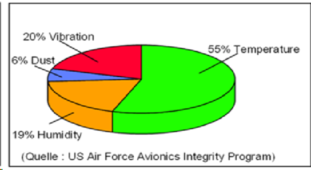
Components and currents heat the PCB (assembly) - but how hot will it get? Are the temperature limits complied with? No data sheet or guideline will tell you.
With TRM (Thermal Risk Management) you are able to calculate the thermal performance of your circuit board before the laboratory test
… and with new TRM 3.7 it's even easier to generate a better temperature forecast. Made easier than with add-ons of the big EDA vendors.
• Import your Gerber, placement, drill files or netlist or set the necessary data manually (see FAQ)
• 3D circuit board model with up to 50 layers
• Update: Easy export and import for ALTIUM users
• NEW: Easy export and import for EAGLE users
• Clearly arranged operation
• Templates and file formats for parameter input
• Can also be used without CAD data - for technologists
• No FEM knowledge required
________________________________________
• Accuracy through physics and geometry
• Heating by components and/or currents
• Environmental conditions. Air cooling, heat sinks and heat sinks, radiation into a vacuum, and much more
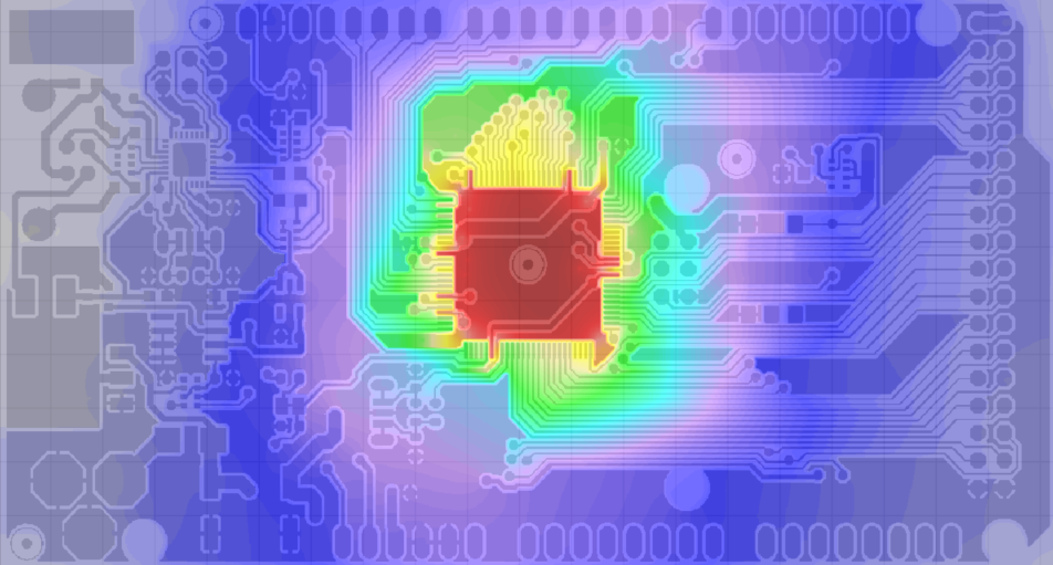
• Virtual thermograms of all layers and prepregs in high resolution
• DC potential distribution and current density in nets
• Steady-state or transient
• Temperature-dependent material data
• Self and mutual inductance (inductance matrix)
• Automatically generated result tables
________________________________________
• Licensing by your server
• Short to moderate computing time on laptop and PC
Request a free Trial installation ar a webdemo .
YouTube: https://www.youtube.com/channel/UCFEwDzwApUYntiE__kJnJJQ